Original Link: https://www.anandtech.com/show/11551/amds-future-in-servers-new-7000-series-cpus-launched-and-epyc-analysis
AMD's Future in Servers: New 7000-Series CPUs Launched and EPYC Analysis
by Ian Cutress on June 20, 2017 4:00 PM EST- Posted in
- CPUs
- AMD
- Enterprise CPUs
- EPYC
- Whitehaven
- 1P
- 2P
The big news out of AMD was the launch of Zen, the new high-performance core that is designed to underpin the product roadmap for the next few generations of products. To much fanfare, AMD launched consumer level parts based on Zen, called Ryzen, earlier this year. There was a lot of discussion in the consumer space about these parts and the competitiveness, and despite the column inches dedicated to it, Ryzen wasn’t designed to be the big story this year. That was left to their server generation of products, which are designed to take a sizeable market share and reinvigorate AMD’s bottom line on the finance sheet. A few weeks ago AMD announced the naming of the new line of enterprise-class processors, called EPYC, and today marks the official launch with configurations up to 32 cores and 64 threads per processor. We also got an insight into several features of the design, including the AMD Infinity Fabric.'
What’s in a Processor?
Today’s announcement of the AMD EPYC product line sees the launch of the top four CPUs, focused primarily at dual socket systems. The full EPYC stack will contain twelve processors, with three for single socket environments, with the rest of the stack being made available at the end of July. It is worth taking a few minutes to look at how these processors look under the hood.
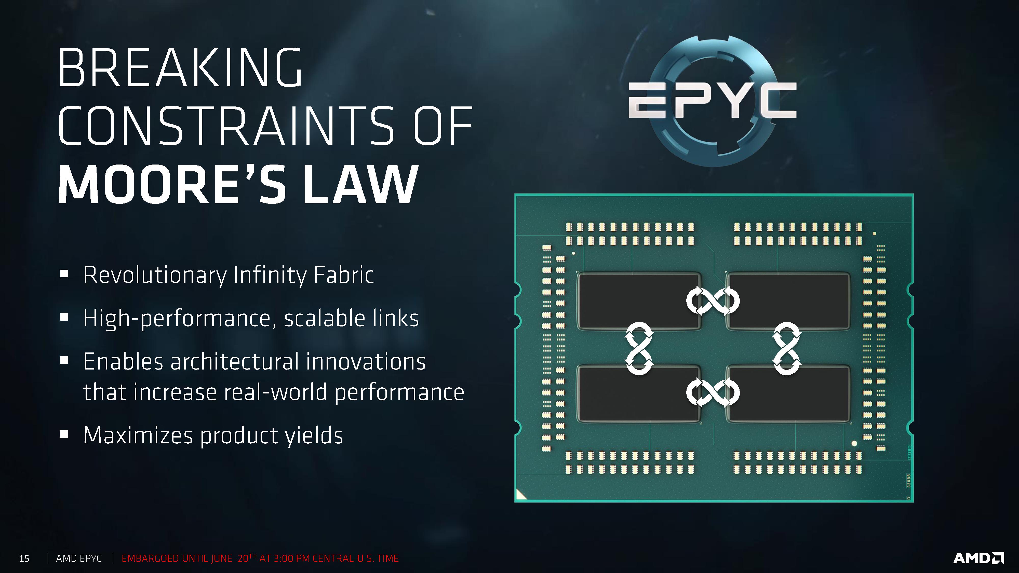
On the package are four silicon dies, each one containing the same 8-core silicon we saw in the AMD Ryzen processors. Each silicon die has two core complexes, each of four cores, and supports two memory channels, giving a total maximum of 32 cores and 8 memory channels on an EPYC processor. The dies are connected by AMD’s newest interconnect, the Infinity Fabric, which plays a key role not only in die-to-die communication but also processor-to-processor communication and within AMD’s new Vega graphics. AMD designed the Infinity Fabric to be modular and scalable in order to support large GPUs and CPUs in the roadmap going forward, and states that within a single package the fabric is overprovisioned to minimize any issues with non-NUMA aware software (more on this later).
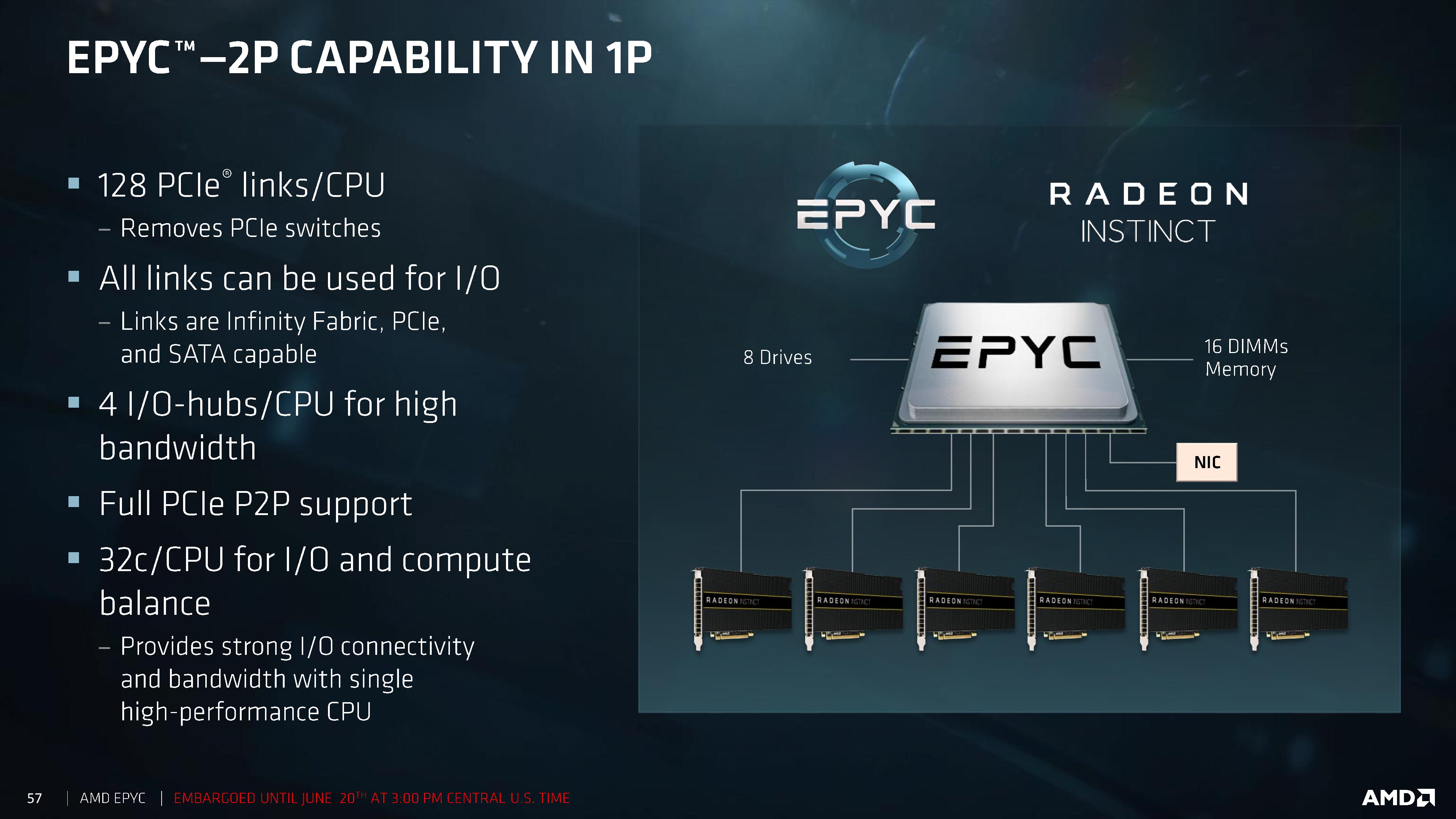
With a total of 8 memory channels, and support for 2 DIMMs per channel, AMD is quoting a 2TB per socket maximum memory support, scaling up to 4TB per system in a dual processor system. Each CPU will support 128 PCIe 3.0 lanes, suitable for six GPUs with full bandwidth support (plus IO) or up to 32 NVMe drives for storage. All the PCIe lanes can be used for IO devices, such as SATA drives or network ports, or as Infinity Fabric connections to other devices. There are also 4 IO hubs per processor for additional storage support.
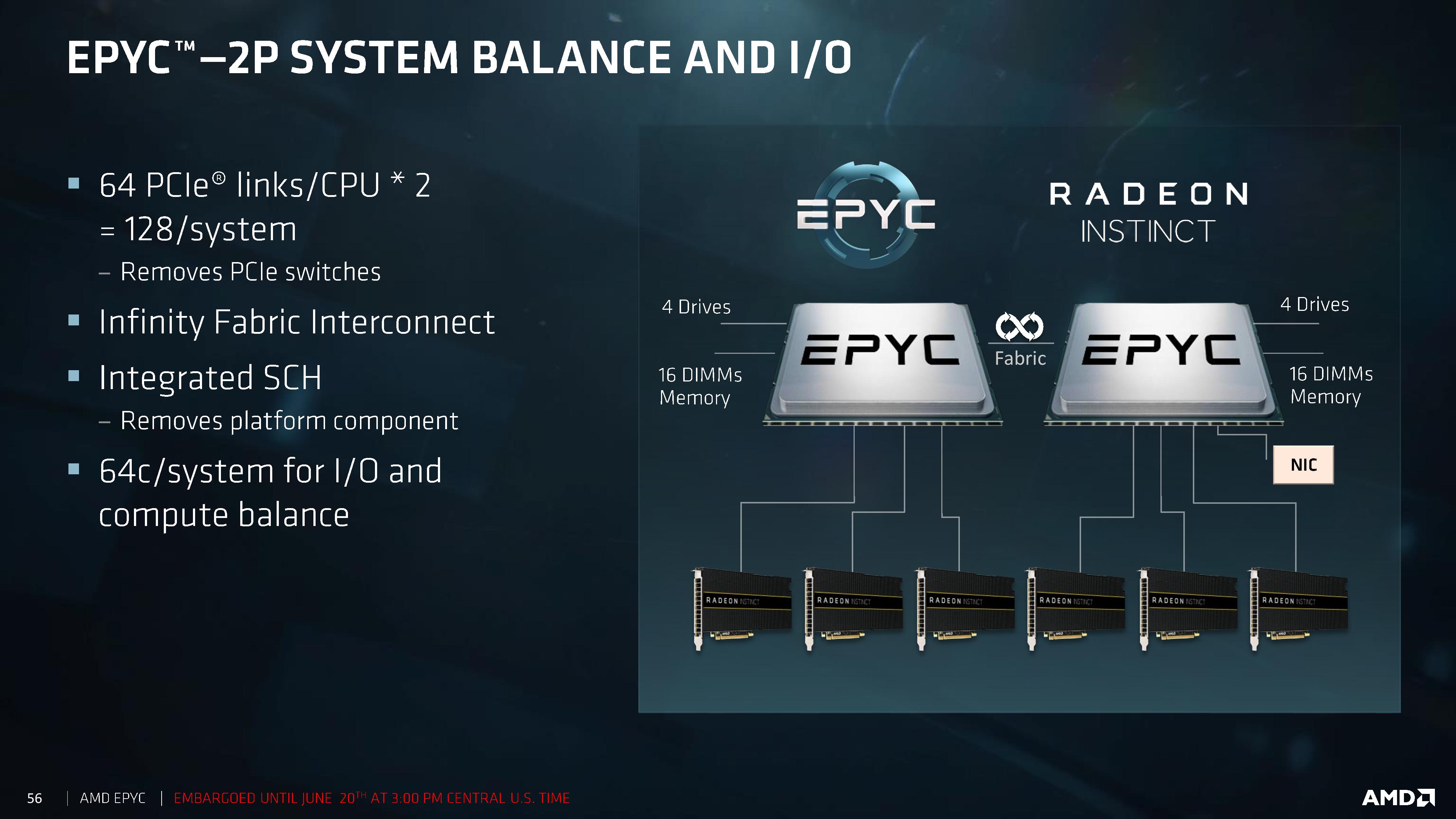
In a dual socket arrangement, each CPU uses 64 PCIe lanes in Infinity Fabric mode to communicate with each other. This means there is still a total of 128 PCIe lanes to be used inside the system, but the total memory support has doubled.
Going BIG and Attacking The Market: All The Cores, Please
AMD is launching a total of nine parts aimed at dual socket use, and three parts for single socket servers. This is consummate with AMD’s strategy of stating that 90-95% of all servers in use today are either single or dual socket, and there will not be quad-socket options on AMD. The goal here is that some of the single socket processor options from AMD could easily replace dual-socket servers for a lower TCO and simplifying the environment by offering more memory and more IO than what is currently on the market.
The new processors from AMD are called the EPYC 7000 series, with names such as EPYC 7301 and EPYC 7551P. The naming of the CPUs is as follows:
EPYC 7551P
- EPYC = Brand
- 7 = 7000 Series
- 30/55 = Dual Digit Number indicative of stack positioning / performance (non-linear)
- 1 = Generation
- P = Single Socket, not present in Dual Socket
So in the future we will see EPYC 7302 processors, or if AMD scales out the design there may be EPYC 5000 processors with fewer silicon dies inside, or EPYC 3000 with a single die but for the EPYC platform socket (obviously, those last two are speculation).
But starting with the 2P processors:
| AMD EPYC Processors (2P) | |||||||||
| Cores Threads |
Frequency (GHz) | L3 | DRAM | PCIe | TDP | Price | |||
| Base | All | Max | |||||||
| EPYC 7601 | 32 / 64 | 2.20 | 2.70 | 3.2 | 64 MB | 8-Ch DDR4 2666 MT/s |
8 x16 128 PCIe |
180W | $4200 |
| EPYC 7551 | 32 / 64 | 2.00 | 2.55 | 3.0 | 180W | >$3400 | |||
| EPYC 7501 | 32 / 64 | 2.00 | 2.60 | 3.0 | 155W/170W | $3400 | |||
| EPYC 7451 | 24 / 48 | 2.30 | 2.90 | 3.2 | 180W | >$2400 | |||
| EPYC 7401 | 24 / 48 | 2.00 | 2.80 | 3.0 | 155W/170W | $1850 | |||
| EPYC 7351 | 16 / 32 | 2.40 | 2.9 | 155W/170W | >$1100 | ||||
| EPYC 7301 | 16 / 32 | 2.20 | 2.7 | 155W/170W | >$800 | ||||
| EPYC 7281 | 16 / 32 | 2.10 | 2.7 | 32 MB | 155W/170W | $650 | |||
| EPYC 7251 | 8 / 16 | 2.10 | 2.9 | 120W | $475 | ||||
All CPUs will have 128 PCIe 3.0 lanes, most have access to all 64MB of L3 cache (except the bottom two), and all support DDR4-2666. AMD continually makes clear that all processors will support all the features involved, and the only differentiation point will be on cores, frequencies, and power.
Sitting on top of the stack is the EPYC 7601, sporting 32 cores with 64 threads, a base frequency of 2.2 GHz, an all-core boost of 2.7 GHz and a boost frequency of 3.2 GHz. Depending on the distribution of software across the cores, the chip should be at the boost frequency when fewer than 12 cores are in use, although other factors such as localized temperature in the core may affect this.
The next two CPUs look the same, but are slightly different. They both have a base frequency of 2.0 GHz, and a peak frequency of 3.0 GHz. Again, the peak frequency should be active when fewer than 12 cores are active. The differences come in the power: the EPYC 7551 is an 180W part, but the EPYC 7501 is listed as 155W/170W. We were told at the AMD Tech Day for EPYC that this 155W/170W listing is due to the fact that this CPU can support DDR4-2400 memory at 155W or DDR4-2666W memory at 170W. So then we have the EPYC 7551 at DDR4-2666 with a 180W TDP, and the EPYC 7501 at DDR4-2666 with a 170W TDP: we’re trying to extract from AMD if there is another difference for this, given that the EPYC 7501 is priced lower and has a lower TDP, but are waiting to hear a response back.
On the 24 core parts, the EPYC 7451 and the EPYC 7401, we have a similar set of differences: the 2.3 GHz part has a base frequency of 2.3 GHz, a maximum boost frequency of 3.2 GHz, and supports 180W, while the 2.0 GHz part has a turbo of 3.0 GHz but has the separate 155W/170W modes again. The EPYC 7401 has an all-core turbo of 2.8 GHz due to having fewer cores, but the threshold for this when in 155W mode is at eight cores. For the 24 core parts, AMD has disabled one core per core complex, leaving 3 per complex (so 6 per die, leading to 24 per chip).
The sixteen-core processors disable two cores per CCX, leading to four per die, but still with the full complement of cache and memory channels. These all have reduced frequencies over the bigger chips, and all come in 155W/170W flavors. These processors will not be out on day one, but we are told to expect OEMs offering systems with these chips in late July.
The final processor is somewhat of an odd-ball. The EPYC 7251 is an eight-core processor, running at a 2.1 GHz base frequency and a 2.9 GHz base frequency, but at 120W. By comparison, Ryzen 7 1700 is an eight-core processor at 3.0/3.7 GHz frequencies but only at 65W, so what is going on here? As mentioned above, all these EPYC 7000-series are based on quad-die designs, so this processor still has the full 700+mm2 of silicon, access to 32MB of L3 cache, access to 8 memory channels up to 2TB of memory, and a full set of PCIe lanes. The chip only has one core active per CCX, meaning that core-to-core latency will be higher than normal, but AMD’s strategy here is one about having a ‘memory optimized’ part. Their justification is that some workloads are not compute bound but DRAM bound. Here is the cheapest CPU in the stack, available for under $400 (or two for under $800), but for software that pays for licenses per core but is memory size bound to require 2TB/4TB, or are GPU bound, then this is the processor to get.
The final three processors are for single socket systems:
| AMD EPYC Processors (1P) | |||||||||
| Cores Threads |
Frequency (GHz) | L3 | DRAM | PCIe | TDP | Price | |||
| Base | All | Max | |||||||
| EPYC 7551P | 32 / 64 | 2.0 | 2.6 | 3.0 | 64 MB | 8-Ch DDR4 2666 MT/s |
8 x16 128 PCIe |
180W | $2100 |
| EPYC 7401P | 24 / 48 | 2.0 | 2.8 | 3.0 | 155W/170W | $1075 | |||
| EPYC 7351P | 16 / 32 | 2.4 | 2.9 | 155W/170W | $750 | ||||
These SKUs mirror the specifications of the 2P counterparts, but have a P in the name.
A Side Note on Performance Claims
In our presentations about the launch, AMD wanted to make two things clear: these parts are designed to offer a lot better raw performance (as defined by SPECint) at every price point, and that these parts aren’t designed to compete with the current E5 v4 processors on the market, but with Skylake-SP. The slide that was presented showed this:

AMD is claiming up to +70% performance for a dual socket system, especially in the ~$800 CPU market which they predict will be the biggest element for sales. Along with this, AMD claimed that for some parts of the market, only one AMD processor will be needed to replace two Intel processors:
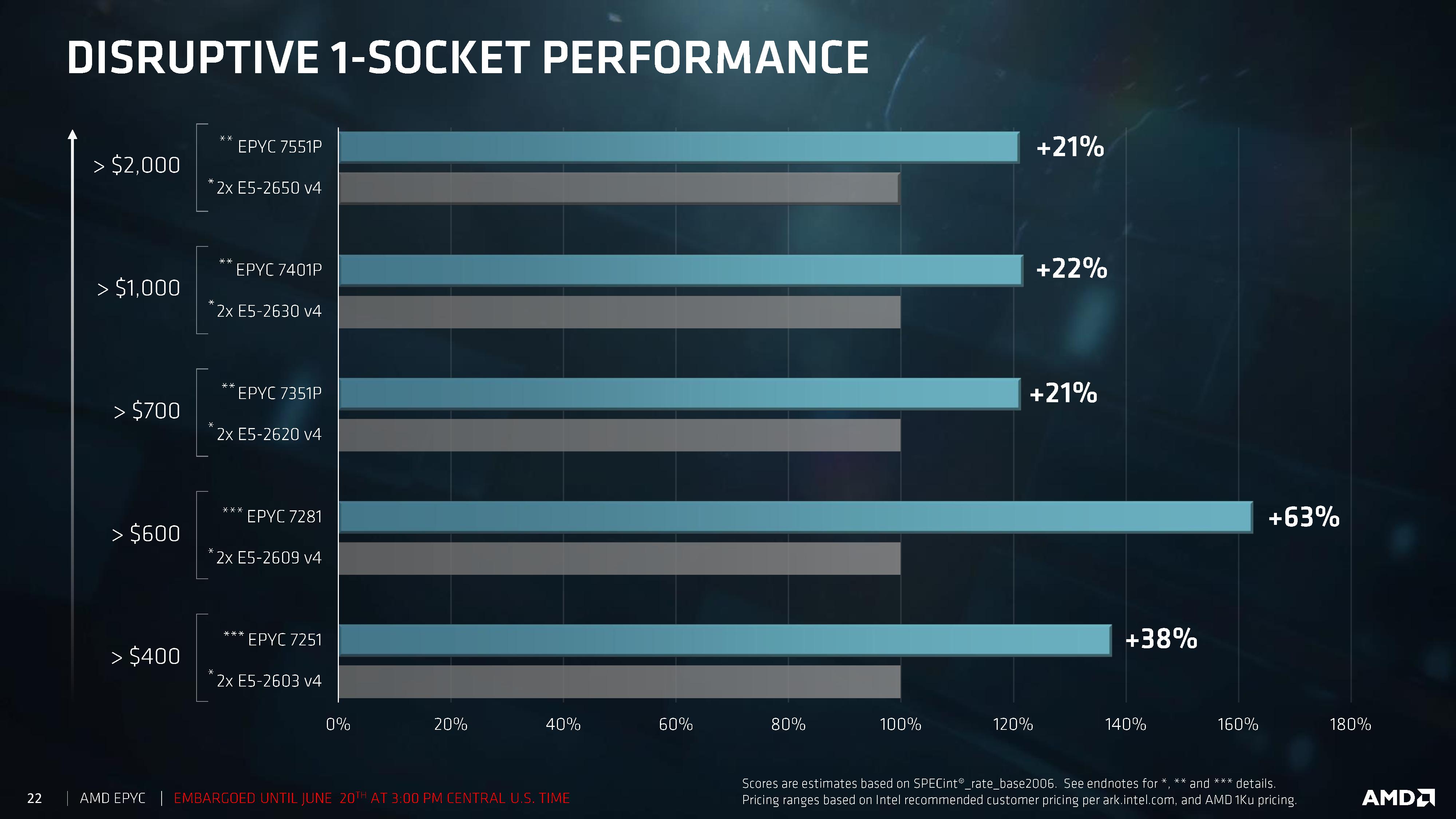
In this case, an EPYC 7281 in single socket mode is listed as having +63% performance (in SPECint) over a dual socket E5-2609v4 system.
I must stress, these are AMD numbers, and vendor numbers should always be taken with a degree of salt due to the risk of cherry picking. Furthermore, as AMD notes in their endnotes, the Intel numbers have been modified. "Scores for these E5 processors extrapolated from test results published at www.spec.org, applying a conversion multiplier to each published score." So we’re waiting to get the chips ourselves to do our own comparison testing.
The next page in this analysis is on NUMA and the Infinity Fabric.
NUMA NUMA IEI: Infinity Fabric Bandwidths
The news about AMD using four Zeppelin dies from Ryzen to form EPYC is not new news, having been shown several times before. However, given the design of the silicon and how the cores communicate, there has been a few worries about how the intra-package communications will be affected by not being a single monolithic die. Beyond that, socket-to-socket communications can also be an issue without sufficient latency and bandwidth.
In a single monolithic die, the latency to access other cores is usually a predictable average, with a regular latency and bandwidth out to the memory channels. Because EPYC has two memory channels per die, if a core needs to access DRAM associated with another die, it adds additional hops and latency to the access, slowing down potential instruction throughput. In the land of dual socket systems, this is known as NUMA: Non-Unified Memory Architecture. The way around a NUMA environment is data locality – keeping the data that a core needs as close as feasibly possible. Solving NUMA is a difficult task, and attempted both at the silicon and software level. Most high-end professional software packages designed for dual-socket systems are NUMA aware, and are designed to compensate for this. The majority of non-high-end software though, is not.
Intra-Socket
With the quad-die design, a single EPYC processor might essentially have four zones for NUMA to occur, based on communication paths. AMD went to specifically address this issue in their design briefings.
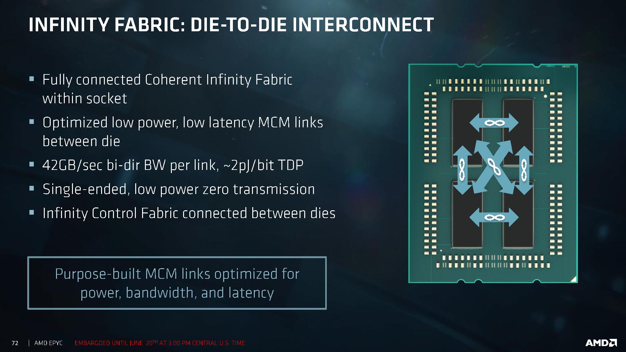
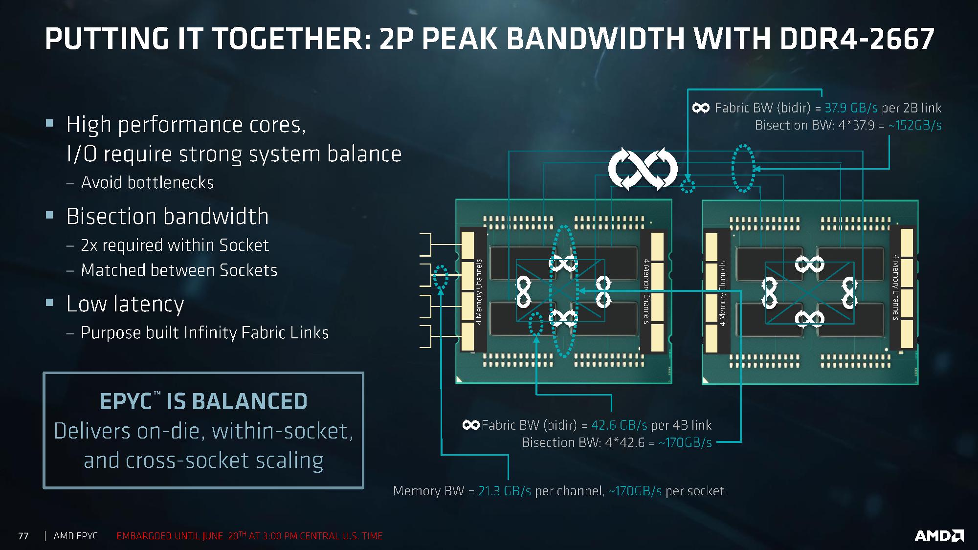
Within a single processor, each of the three dies is directly linked to each other through the Infinity Fabric, so only one hop is ever needed when data goes off-die. The connectivity here is set at a bidirectional 42.6 GB/sec per link, at around an average energy of ~2 pJ per bit (or 0.672W per link, 0.336W per die per link, totaling 4.032W for the chip). It is worth noting that Intel’s eDRAM for Broadwell was set as a 50 GB/s bidirectional link, so in essence moving off die in EPYC has a slightly slower bandwidth than Crystalwell. With a total of six links within the silicon, that provides a total of 2 terabits per second of data movement, although AMD didn’t state what the bottlenecks or latency values were.
Inter-Socket
Socket-to-socket communication is designed at the die level, rather than going through a singular interface. One die in each processor is linked to the same die in the other processor, meaning that for the worst-case scenario data has to make two hops to reach a core or memory controller on the other side of the system. Each link has a bidirectional 37.9 GB/s bandwidth, which is only slightly less than the intra-socket communication bandwidth, although we would expect socket-to-socket to have a slightly higher latency based on distance. AMD has not shared latency numbers at this time.
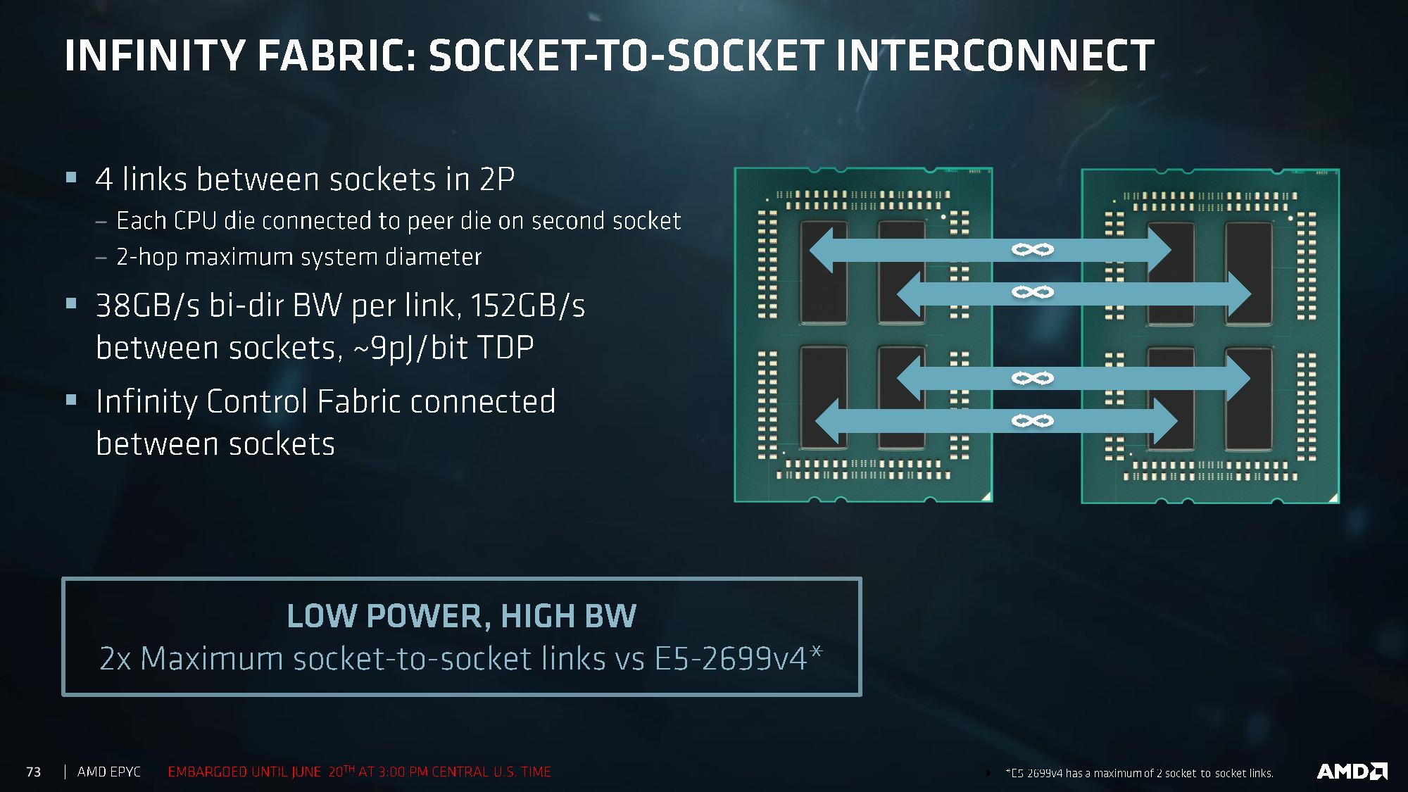
At 37.9 GB/s per link, this totals 152 GB/s between sockets, which AMD states runs at an average of 9 pJ per bit. So at full speed, this link will consume 10.94W between the two sockets, or 5.48W per processor and 1.368W per silicon die.
Totaling the 1.368W per die for socket-to-socket plus 3*0.336W per die for intra-socket communications, the Infinity Fabric can consume 2.376W per silicon die on average when going at full speed.
Infinity Fabric Latency
AMD has not provided Infinity Fabric numbers for latency. We are waiting on information, but this is likely going to be a critical answer for some software packages. Based on testing done by PC Perspective, we already know some latency numbers within a single Zeppelin die from the Ryzen platform. This allows us to fill in the following table showing how long it takes to ping another core:
| EPYC (Naples) Thread Ping Connections | ||
| Latency | Bandwidth | |
| Within A Core | 26 ns | - |
| Core-to-Core, Same CCX | 42 ns | - |
| Core-to-Core, Different CCX, Same Die | 142 ns | - |
| Die-to-Die, Same Package | ? | 42.6 GB/s |
| Die-to-Die, Different Socket, One Hop | ? | 37.9 GB/s |
| Die-to-Die, Different Socket, Two Hops | ? | 37.9 GB/s |
| Core to DRAM, Same Die | ? | 42.6 GB/s |
| Core to DRAM, Different Die | ? | 42.6 GB/s |
| Core to DRAM, Different Socket, One Hop | ? | 37.9 GB/s |
| Core to DRAM, Different Socket, Two Hops | ? | 37.9 GB/s |
PCIe Bandwidth
Each Zeppelin die can create two PCIe 3.0 x16 links, which means a full EPYC processor is capable of eight x16 links totaling the 128 PCIe lanes presented earlier. AMD has designed these links such that they can support both PCIe at 8 GT/s and Infinity Fabric at 10.6 GT/s, although in PCIe mode this means 32GB/s of bidirectional bandwidth per link, suitable for 256GB/s per socket. One of AMD’s proposed benefits here is link bifurcation support:
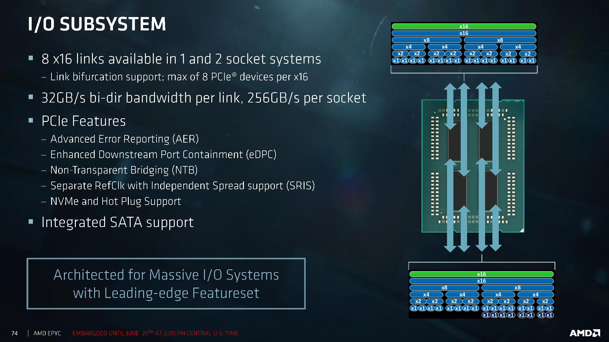
Each x16 link can support Infinity Fabric (green), PCIe (blue) and SATA (dark blue). PCIe can be bifurcated all the way down to sets of x1, although there will be a limit of 8 PCIe devices per x16 link, but this becomes a mix and match game: x8 + x4 + x2 + x1 + x1 + x1 + x1 becomes entirely valid for a single x16 link, and each CPU has eight of these such links. For the SATA connectivity, each x16 link can support 8 SATA drives as a result. If you really want 64 devices per processor, welcome to your platform without buying PCIe switches. AMD states that as an NVMe implementation, supporting 32 NVMe devices is going to be no sweat for an EPYC system.
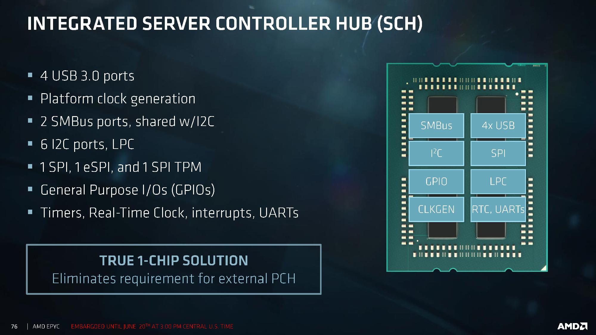
This also relates to the Sever Controller Hub, which acts as part of the design offering four USB 3.0 ports, SMBus, I2C, SPI, eSPI, TPM, GPIOs, timers and UARTs.
Combining The Bandwidth
Altogether, AMD is stating that they are relatively unconcerned about NUMA related issues, with bandwidth between dies and between sockets being relatively similar. It is worth noting that the 42.6 GB/s die-to-die bandwidth is identical to the dual-channel memory bandwidth quoted per die:
Time will tell if these become bottlenecks. Latency numbers please, I’d love to fill in that table above.
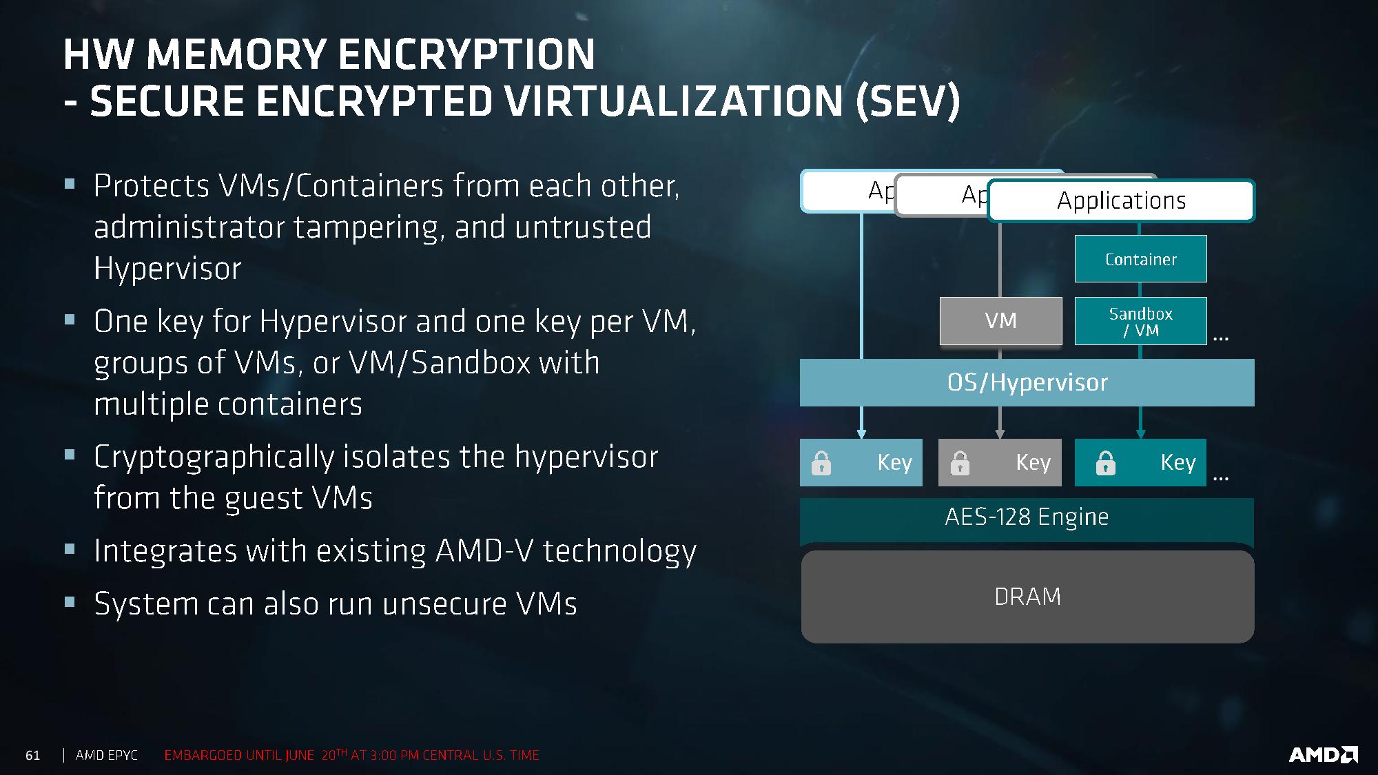
With recent fears about security, and given that these processors are aiming to go to the Enterprise space, AMD had to dedicate some time to explaining how secure the new platform is. AMD has had its Secure Processor in several CPUs at this point: a 32-bit ARM Cortex-A5 acting as a microcontroller that runs a secure OS/kernel with secure off-chip storage for firmware and data – this helps provide cryptographic functionality for secure key generation and key management. This starts with hardware validated boot (TPM), but includes Secure Memory Encryption and Secure Encrypted Virtualization.
Encryption starts at the DRAM level, with an AES-128 engine directly attached to the MMU. This is designed to protect against physical memory attacks, with each VM and Hypervisor able to generate a separate key for their environment. The OS or Hypervisor can choose which pages to encrypt via page tables, and the DMA engines can provide support for external devices such as network storage and graphics cards to access encrypted pages.
Because each VM or container can obtain its own encryption key, this isolates them from each other, protecting against cross-contamination. It also allows unencrypted VMs to run alongside encrypted ones, removing the all-or-nothing scenario. The keys are transparent to the VMs themselves, managed by the protected hypervisor. It all integrates with existing AMD-V technology.
Alongside this are direct RAS features in the core, with the L1 data cache using SEC-DED ECC and L2/L3 caches using DEC-TED ECC. The DRAM support involves x4 DRAM device failure correction with addr/cmd parity and write CRC with replay. Data poisoning is handled with reporting and a machine check recovery mode. The Infinity Fabric between dies and between sockets is also link-packet CRC backed with retry.
One element that was not discussed is live VM migration across encrypted environments. We fully suspect that an AMD-to-AMD live migration be feasible, although an AMD-to-Intel or Intel-to-AMD will have issues, given that each microarchitecture has unique implementations of certain commands.
Power
As with the Ryzen parts, EPYC will support 0.25x multipliers for P-state jumps of 25 MHz. With sufficient cooling, different workloads will be able to move between the base frequency and the maximum boost frequency in these jumps – AMD states that by offering smaller jumps it allows for smoother transitions rather than locking PLLs to move straight up and down, providing a more predictable performance implementation. This links into AMD’s new strategy of performance determinism vs power determinism.
Each of the EPYC CPUs include two new modes, one based on power and one based on performance. When a system configured at boot time to a specific maximum power, performance may vary based on the environment but the power is ultimately limited at the high end. For performance, the frequency is guaranteed, but not the power. This enables AMD customers to plan in advance without worrying about how different processors perform with regards voltage/frequency/leakage, or helps provide deterministic performance in all environments. This is done at the system level at boot time, so all VMs/containers on a system will be affected by this.
This extends into selectable power limits. For EPYC, AMD is offering the ability to run processors at a lower or higher TDP than out of the box – most users are likely familiar with Intel’s cTDP Up and cTDP Down modes on the mobile processors, and this feature by AMD is somewhat similar. As a result, the TDP limits given at the start of this piece can go down 15W or up 20W:
| EPYC TDP Modes | ||
| Low TDP | Regular TDP | High TDP |
| 155W | 180W | 200W |
| 140W | 155W | 175W |
| 105W | 120W | - |
The sole 120W processor at this point is the 8-core EPYC 7251 which is geared towards memory limited workloads that pay licenses per core, hence why it does not get a higher power band to work towards.
Workload-Aware Power Management
One of AMD’s points about the sort of workloads that might be run on EPYC is that sporadic tasks are sometimes hard to judge, or are not latency sensitive. In a non-latency sensitive environment, in order to conserve power, the CPU could spread the workload out across more cores at a lower frequency. We’ve seen this sort of policy before on Intel’s Skylake and up processors, going so far as duty cycling at the efficiency point to conserve power, or in the mobile space. AMD is bringing this to the EPYC line as well.

Rather than staying at the high frequency and continually powering up and down, by reducing the frequency such the cores are active longer, latency is traded for power efficiency. AMD is claiming up to a 10% perf-per-Watt improvement with this feature.
Frequency and voltage can be adjusted for each core independently, helping drive this feature. The silicon implements per-core linear regulators that work with the onboard sensor control to adjust the AVFS for the workload and the environment. We are told that this helps reduce the variability from core-to-core and chip-to-chip, with regulation supported with 2mV accuracy. We’ve seen some of this in Carrizo and Bristol Ridge already, although we are told that the goal for per-core VDO was always meant to be EPYC.
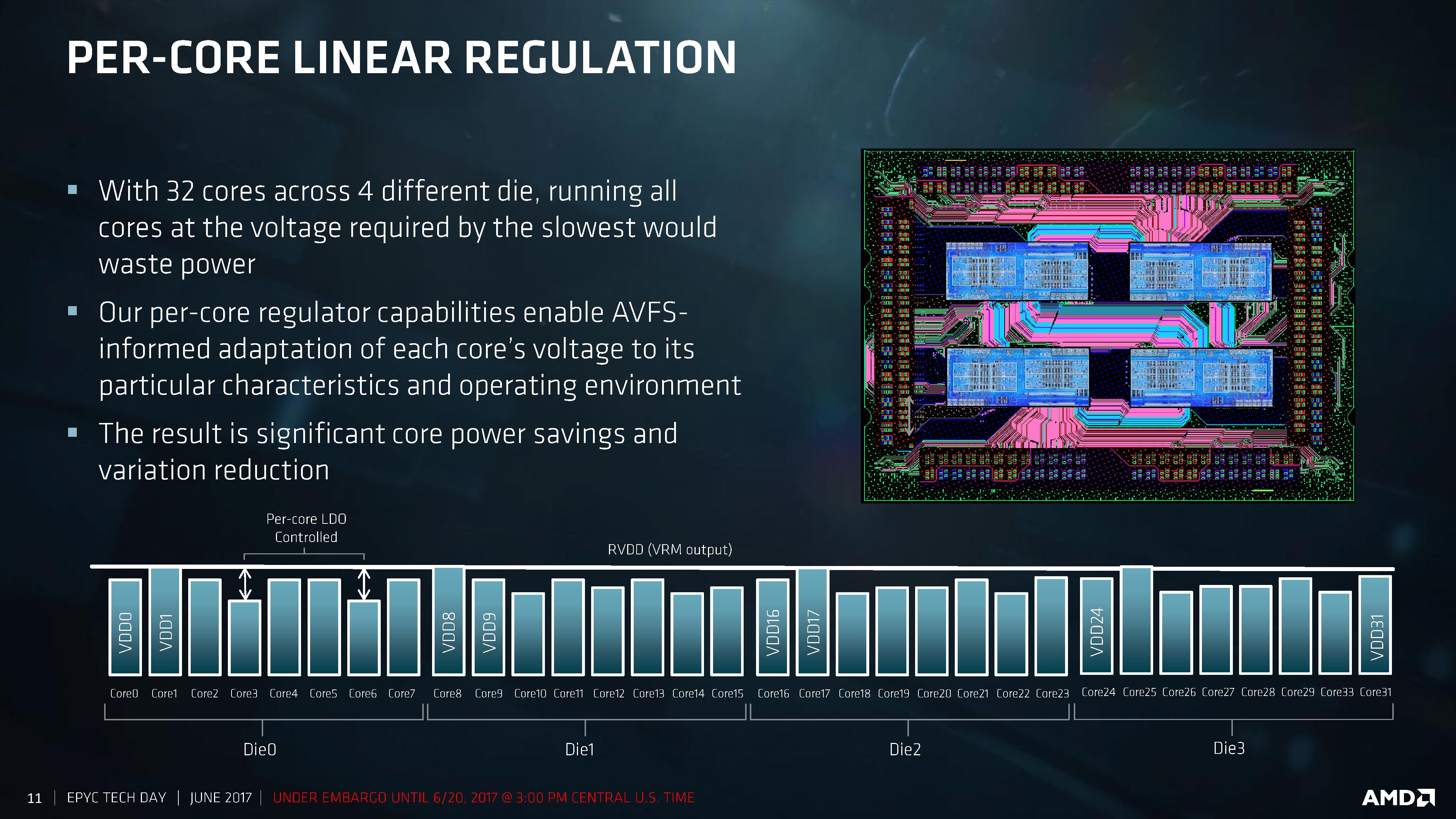
This can not only happen on the core, but also on the Infinity Fabric links between the CPU dies or between the sockets. By modulating the link width and analyzing traffic patterns, AMD claims another 8% perf-per-Watt for socket-to-socket communications.
Performance-Per-Watt Claims
For the EPYC system, AMD is claiming power efficiency results in terms of SPEC, compiled on GCC 6.2:
| AMD Claims 2P EPYC 7601 vs 2P E5-2699A V4 |
||
| SPECint | SPECfp | |
| Performance | 1.47x | 1.75x |
| Average Power | 0.96x | 0.99x |
| Total System Level Energy | 0.88x | 0.78x |
| Overall Perf/Watt | 1.54x | 1.76x |
Comparing a 2P high-end EPYC 7601 server against Intel’s current best 2P E5-2699A v4 arrangement, AMD is claiming a 1.54x perf/watt for integer performance and 1.76x perf/watt on floating point performance, giving more performance for a lower average power resulting in overall power gains. Again, we cannot confirm these numbers, so we look forward to testing.
AMD’s Reach and Ecosystem
As mentioned at the top of the piece, the big launch for AMD this year is the server platform. EPYC has an opportunity to reinvigorate AMD’s bottom line to the tune of several billion dollars a year, if they can get traction in the market. Depending on which Analyst you speak to, some are predicting anywhere from a 5% to a 25% gain in market share for AMD, into a ~$25B total addressable market. Given AMD’s worth, that would mean that the balance sheet in a few years might look as if 80% of it is provided by the server team.
As part of the launch today, AMD is announcing partners working with them to optimize the platform for various workloads. Sources say that this includes all the major cloud providers, as well as all the major OEMs. We saw several demo systems at the launch event with partners as well, such as HPE and Dell.
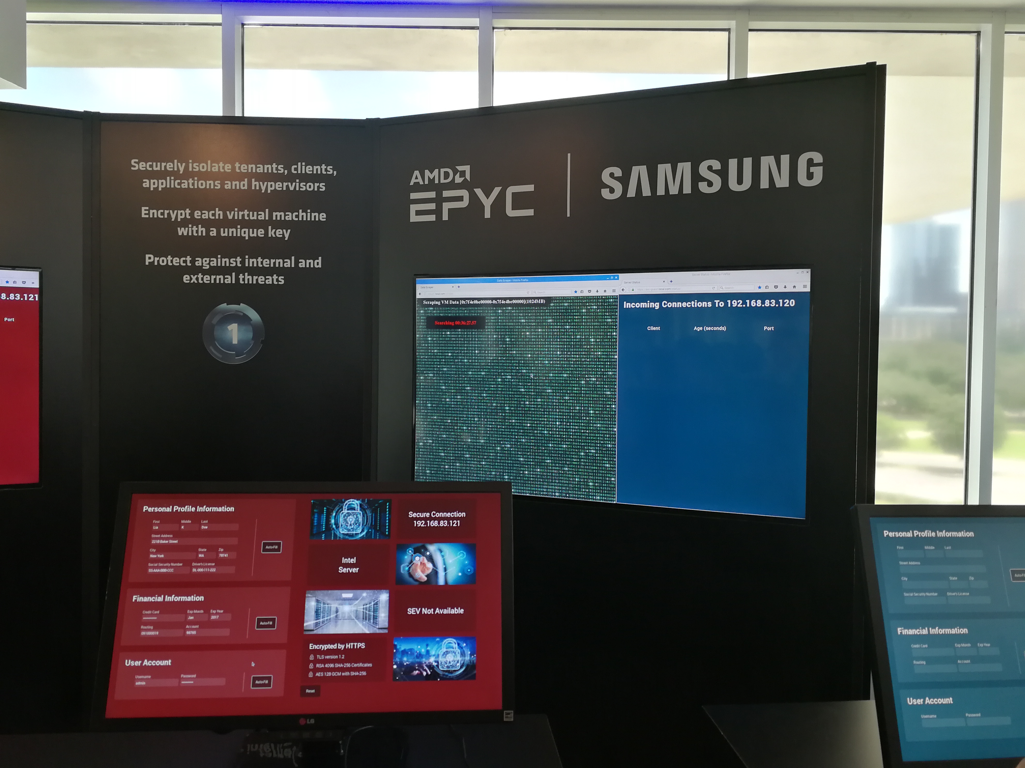
Using SME/SVE with Samsung
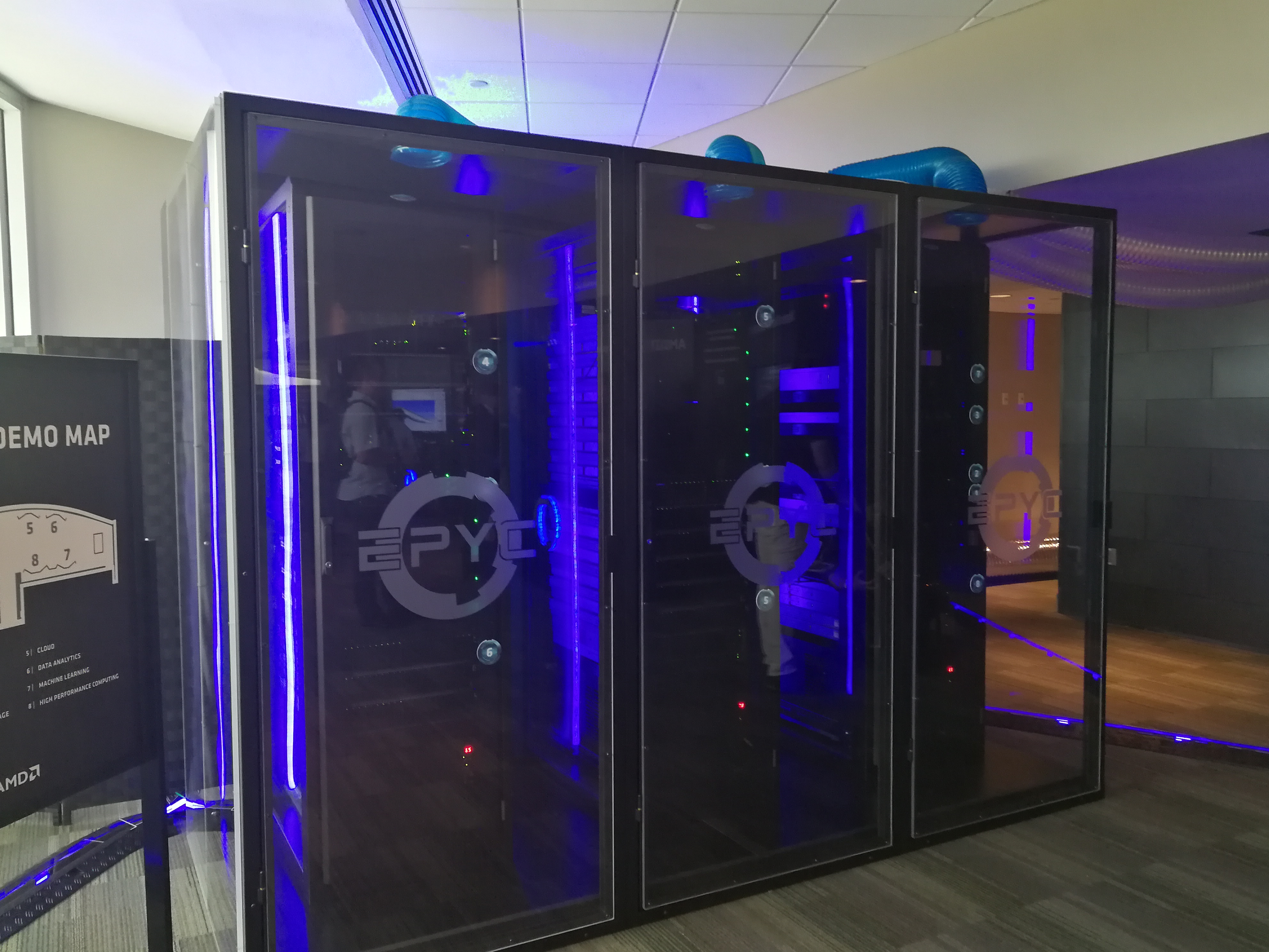
The variety of internal systems used by AMD for the demonstrations (some Dell/HP logos)
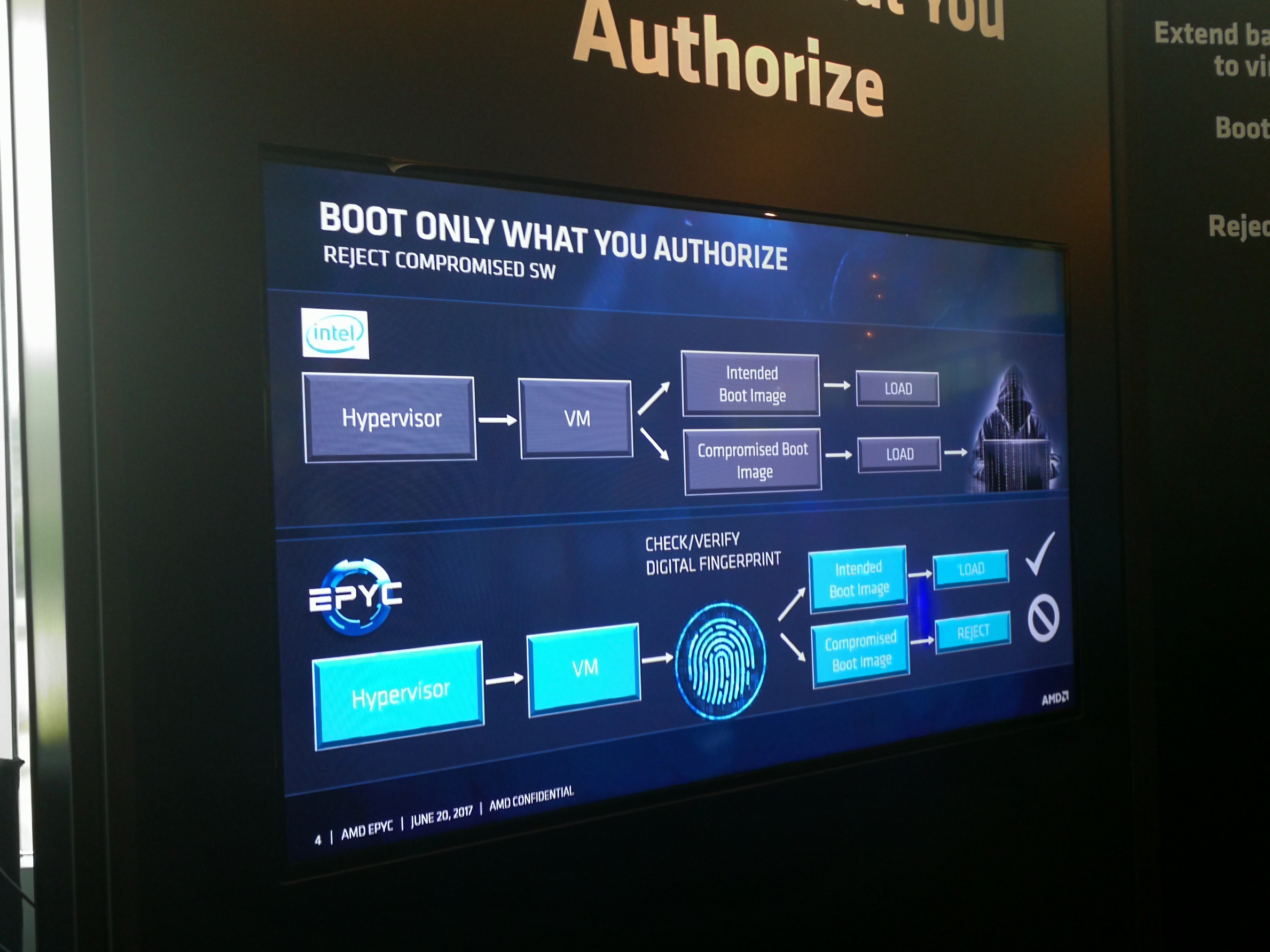
Security Demonstration
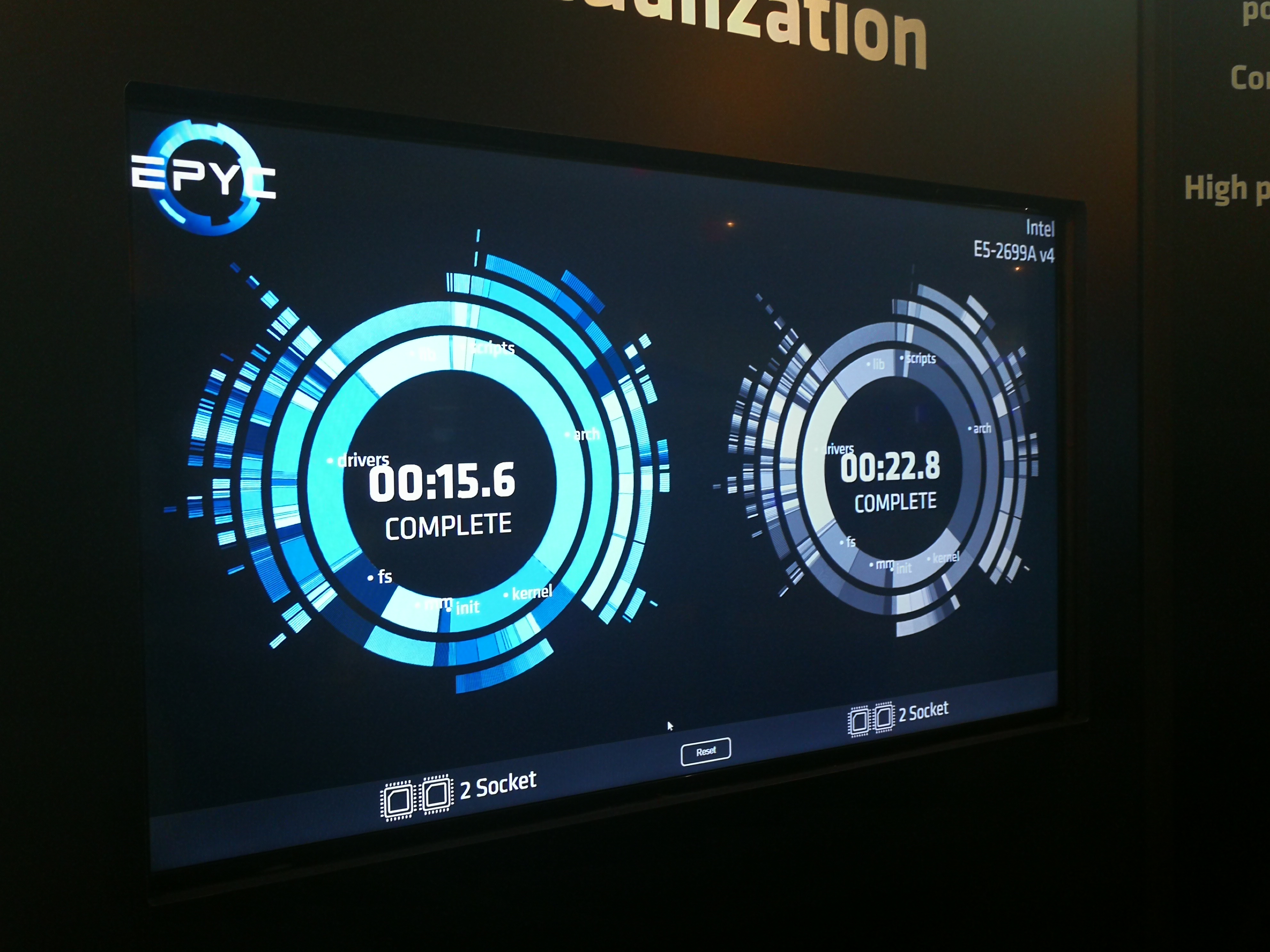
Using 8 VMs to compile the Linux Kernel in one go on AMD vs Intel 2P systems
Of course, the big question is if AMD is actually getting in significant orders for processors. Nothing is public on that yet, and we are told that they are likely to be nearer the end of the year. We are eagerly waiting to test the processors when our review systems arrive, and we will provide our performance breakdown soon.


